NUS deepens AI push in semiconductor R&D with Applied Materials
The collaboration connects research lab optimisation with talent pipeline for industry needs.
The National University of Singapore (NUS) is working with Applied Materials to use artificial intelligence (AI) to speed up semiconductor process development whilst also building a specialised talent pipeline for AI-driven manufacturing.
The collaboration will focus on using AI within the Applied Materials–NUS Advanced Materials Corporate Lab to reduce the trial-and-error cycles involved in developing and optimising semiconductor materials and processes, according to a joint statement.
The partners said AI models will be trained on experimental and equipment-generated data to help identify and prioritise the next set of experiments.
The aim is to support faster iteration from laboratory research to production environments by improving how process conditions and material behaviours are evaluated, according to the statement.
In parallel, NUS will introduce a new postgraduate specialisation in “Applied AI for Materials and Process Engineering” under its Master of Science in Semiconductor Technology and Operations programme from August 2026.
The course will cover machine learning, computer vision, and generative AI, with applications in semiconductor manufacturing such as defect detection, predictive maintenance, and yield optimisation.
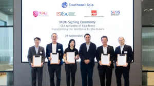
The collaboration was formalised through a memorandum of understanding signed by NUS deputy president for academic affairs and provost professor Aaron Thean and Applied Materials regional president for Southeast Asia Brian Tan.
The signing took place alongside the opening of Applied Materials’ Tampines campus.
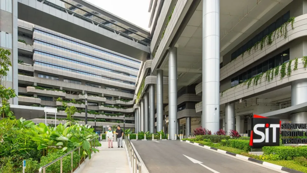
The initiatives are supported by a $3m endowed gift from Applied Materials and were launched in conjunction with a separate partnership with the Singapore Institute of Technology (SIT), which includes industry-based professorship and scholarship programmes for engineering students.
Thean said the collaboration reflects efforts to integrate AI more directly into both semiconductor research and training.
Applied Materials semiconductor products group president Prabu Raja said combining academic research with industrial data can help reduce development cycles between lab and manufacturing environments.
The Corporate Lab, established in 2018 and expanded in 2024, brings together applied chemistry, materials science, and semiconductor process engineering research.
The partners said the AI system under development will combine simulation and experimental data to recommend subsequent tests, creating a feedback loop aimed at improving process efficiency.
NUS said the new specialisation is intended to prepare graduates for roles at the intersection of artificial intelligence and semiconductor manufacturing as demand for data-driven engineering skills increases.



















 Read Here
 Advertise
 Sign Up